
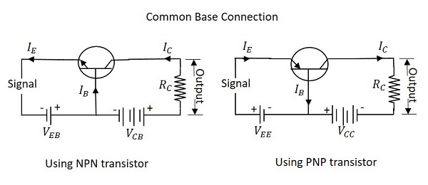
COMMON BASE CONFIGURATION
This is also called as Grounded-base configuration. since the base is common to the input and output circuits.For a p-n-p transistor the largest current components are due to holes. since holes flow from the emitter to the collector and down toward ground out of the base terminal, then , referring to polarity conventions as below..
We may completely describe the transistor by the following two relations, which give the input voltage Veb and output current Ic in terms of the output voltage Vcb and input current Ie:
Veb = f(Vcb,Ie)
Ic=f(Vcb,Ie)

The curves of above figure are known as the output, or collector , static characteristics.
It is customary to plot that along the abscissa and to the right that polarity of Vcb which reverse biases the collector junction even if this polarity is negative. the collector to base diode is normally biased in the reverse direction. If Ie=0, the collector current is Ic=Ic0 ; for other values of Ie, the output diode reverse current is augmented by the fraction of the input diode forward current which reaches the collector. note also that Ico is negative for a p-n-p transistor and positive for n-p-n transistor.
 |
In the active region the input diode is biased in the forward direction. The input characteristics of above figure represent simply the forward characteristics of the emitter-to-base diode for various collector voltages. a noteworthy feature of the input characteristics is that there exists a cutin, offset, or threshold voltage Vt, below which the emitter current is very small.
If we consider the fact that an increase in magnitude of collector voltage will , by early effect , cause the emitter current to increase, with Veb held constant.Thus the curves shift downward as Vcb increases.
The curve with the collector open represents the characteristics of the forward biased emitter diode. when the collector is shorted to the base , the emitter current increases for a given Veb since the collector now removes minority carriers from the base, and hence the base can attract more holes fom the emitter. This means that the curve with VCB=0 is shifted downward from the collector characteristic marked Vcb open.
Early effect:
An increase in magnitude of collector voltage increases the space charge width at the output junction diode.We see that such action causes the effective base width W to decrease, a phenomenon is known as EARLY EFFECT.
This decrease in the base W has two consequences : first there is less chance for recombination within the base region.Hence the transport factor β and also ∝, increase with an increase in the magnitude of the collector junction voltage.Second, the charge gradient is increased with in the base, and consequently, the current of minority carriers injected across the emitter junction increases.


No comments