
COMMON EMITTER CONFIGURATION
This is also called as GROUND-EMITTER configuration. The input current and the output voltage are taken as the independent variables, whereas the input voltage and output current are the dependent variables.
we may write,
Vbe= f(Vce,Ib)............1
Ic= f(Vce,Ib).................2
In the above equations, first equation will represent input characteristic curves and second equation represents the family of output characteristic curves.
 |
| CE configuration |
INPUT & OUTPUT CHARACTERISTICS:
 |
| P-N-P TRANSISTOR CE configuration |
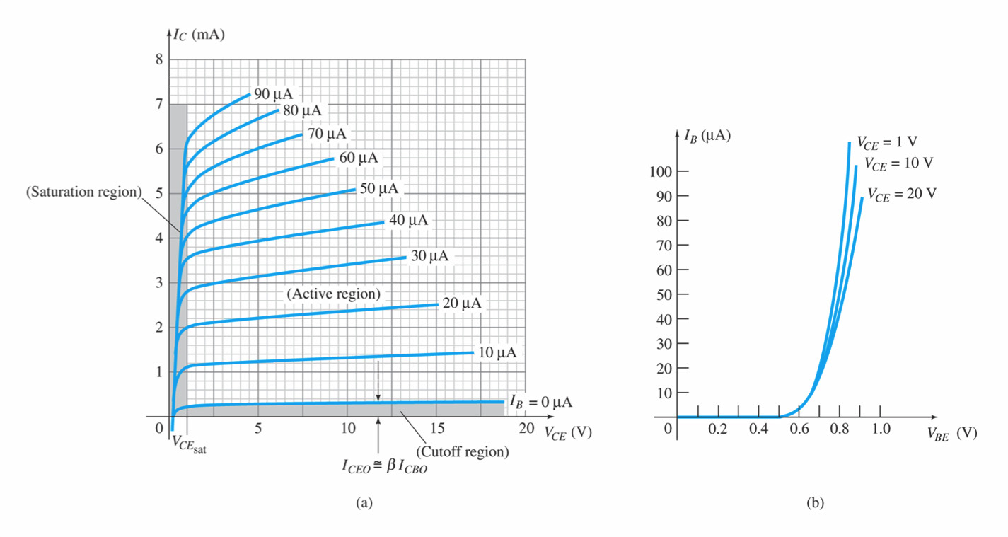
In the above graphs the fig(a) shows output characteristics and fig(b) shows input characteristics.
Common Emitter Curves:
Common Emitter Curves:
The common emitter configuration of BJT is shown in fig. 1.
Fig. 1In C.E. configuration the emitter is made common to the input and output. It is also referred to as grounded emitter configuration. It is most commonly used configuration. In this, base current and output voltages are taken as impendent parameters and input voltage and output current as dependent parametersVBE = f1 ( IB, VCE )
IC = f2( IB, VCE )

Input Characteristic:
The curve between IB and VBE for different values of VCE are shown in fig. 2. Since the base emitter junction of a transistor is a diode, therefore the characteristic is similar to diode one. With higher values of VCE collector gathers slightly more electrons and therefore base current reduces. Normally this effect is neglected. (Early effect). When collector is shorted with emitter then the input characteristic is the characteristic of a forward biased diode when VBE is zero and IBis also zero.

In fig(a), For fixed value of IB, IC is not varying much dependent on VCE but slopes are greater than CE characteristic. The output characteristics can again be divided into three parts.
Large Signal Current Gain βdc :-Fig. 3(1) Active Region:In this region collector junction is reverse biased and emitter junction is forward biased. It is the area to the right of VCE = 0.5 V and above IB= 0. In this region transistor current responds most sensitively to IB. If transistor is to be used as an amplifier, it must operate in this region.If adc is truly constant then IC would be independent of VCE. But because of early effect, adc increases by 0.1% (0.001) e.g. from 0.995 to 0.996 as VCE increases from a few volts to 10V. Then bdc increases from 0.995 / (1-0.995) = 200 to 0.996 / (1-0.996) = 250 or about 25%. This shows that small change in a reflects large change in b. Therefore the curves are subjected to large variations for the same type of transistors.(2) Cut Off:Cut off in a transistor is given by IB = 0, IC= ICO. A transistor is not at cut off if the base current is simply reduced to zero (open circuited) under this condition,IC = IE= ICO / ( 1-αdc) = ICEOThe actual collector current with base open is designated as ICEO. Since even in the neighborhood of cut off, a dc may be as large as 0.9 for Ge, then IC=10 ICO(approximately), at zero base current. Accordingly in order to cut off transistor it is not enough to reduce IB to zero, but it is necessary to reverse bias the emitter junction slightly. It is found that reverse voltage of 0.1 V is sufficient for cut off a transistor. In Si, the a dc is very nearly equal to zero, therefore, IC = ICO. Hence even with IB= 0, IC= IE= ICO so that transistor is very close to cut off.In summary, cut off means IE = 0, IC = ICO, IB = -IC = -ICO , and VBE is a reverse voltage whose magnitude is of the order of 0.1 V for Ge and 0 V for Si.Reverse Collector Saturation Current ICBO:When in a physical transistor emitter current is reduced to zero, then the collector current is known as ICBO (approximately equal to ICO). Reverse collector saturation current ICBO also varies with temperature, avalanche multiplication and variability from sample to sample. Consider the circuit shown in fig. 4. VBB is the reverse voltage applied to reduce the emitter current to zero.IE = 0, IB = -ICBOIf we require, VBE = - 0.1 VThen - VBB + ICBO RB < - 0.1 VFig. 4If RB = 100 K, ICBO = 100 m A, Then VBB must be 10.1 Volts. Hence transistor must be capable to withstand this reverse voltage before breakdown voltage exceeds.(3).Saturation Region:In this region both the diodes are forward biased by at least cut in voltage. Since the voltage VBE and VBC across a forward is approximately 0.7 V therefore, VCE = VCB + VBE = - VBC + VBE is also few tenths of volts. Hence saturation region is very close to zero voltage axis, where all the current rapidly reduces to zero. In this region the transistor collector current is approximately given by VCC / R C and independent of base current. Normal transistor action is last and it acts like a small ohmic resistance.


The ratio Ic / IB is defined as transfer ratio or large signal current gain bdcWhere IC is the collector current and IB is the base current. The bdc is an indication if how well the transistor works. The typical value of bdc varies from 50 to 300.In terms of h parameters, b dc is known as dc current gain and in designated hfE ( b dc = hfE). Knowing the maximum collector current and bdc the minimum base current can be found which will be needed to saturate the transistor.This expression of bdc is defined neglecting reverse leakage current (ICO).Taking reverse leakage current (ICO) into account, the expression for the bdc can be obtained as follows:bdc in terms of adc is given bySince, ICO = ICBOCut off of a transistor means IE = 0, then IC= ICBO and IB = - ICBO. Therefore, the above expression bdc gives the collector current increment to the base current change form cut off to IB and hence it represents the large signal current gain of all common emitter transistor.


No comments