GaN: From Watts to Kilowatts
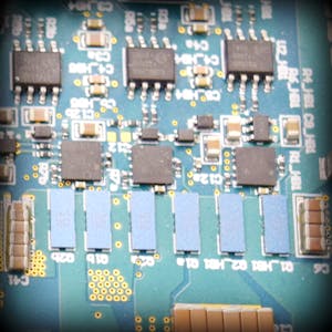
GaN FETs have enabled high-frequency power converter designs that are much higher in power density, smaller in size, and are light-weight due to superior switching characteristics and lack of reverse recovery losses. To get full benefit of GaN’s fast switching speeds, the power loop inductance needs to be minimized. This necessitates careful PCB layout as well as very low inductance package for GaN FETs. TI’s LMG341XRxxx family uses 8-mm × 8-mm low inductance bottom side cooled QFN package for switching speeds of greater than 100 V/ns. A good thermal design is important for power electronic converters. An ideal heat transfer should provide good thermal conductivity with minimum thermal resistance in the heat flow path.


No comments