
P-N Junction Diode
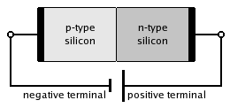
Constructional details of P-N diode:
 |
| P-N diode |
P-N junction is formed by using a p-type and n-type semi conducting materials. the p-type material has holes as majority carriers and n-type material has free electrons as it's majority carriers. The junction is formed when these two materials connected together. The diode always conducts in one direction of current flow and refuses to conduct in other direction. why this happens will be known in further concepts.
The p-n junction is a building block for construction of Diodes,Transistors,Amplifiers,integrated circuits etc. A Schottky junction is a special case of a p–n junction, where metal serves the role of the p-type semiconductor. That'y we have to learn much precise about this concept.
Properties:
 |
| diode details |
We have the conductivity caused by holes in p-type semiconductor and as well as electrons in n-type semiconductor. But the depletion region itself is a non conductive region in the p-n junction diode. the region is formed when we attached p and n type materials. The conductivity of current is occurs in one direction that will be known as FORWARD bias. And there is flow of current in another region which is called as REVERSE bias region. These regions formed by the voltage source polarity we chose with respect to the junction diode polarity as explained below.
At Equilibrium Condition(Zero Bias):
 |
| A p–n junction in thermal equilibrium with zero-bias voltage applied. Electron and hole concentration are reported with blue and red lines, respectively. Gray regions are charge-neutral. Light-red zone is positively charged. Light-blue zone is negatively charged. The electric field is shown on the bottom, the electrostatic force on electrons and holes and the direction in which the diffusion tends to move electrons and holes. (The log concentration curves should actually be smoother with slope varying with field strength.) |
With out applying any external voltage the diode attains an equilibrium condition in which a potential barrier is formed at junction. The process of diffusion can be caused to the equilibrium condition. The charge carriers are moved from high concentration area to low concentration regions is known by Diffusion.
 |
| characteristics of p-n diode at equilibrium condition |
| diode bias conditions |
Forward bias:
In forward bias condition the positive terminal of voltage source is connected to the p type and negative terminal is connected to the n type material of diode.
With a battery connected this way, the holes in the p-type region and the electrons in the n-type region are pushed toward the junction and start to neutralize the depletion zone, reducing its width. The positive potential applied to the p-type material repels the holes, while the negative potential applied to the n-type material repels the electrons. The change in potential between the p side and the n side decreases or switches sign. With increasing forward-bias voltage, the depletion zone eventually becomes thin enough that the zone's electric field cannot counteract charge carrier motion across the p–n junction, which as a consequence reduces electrical resistance. Electrons that cross the p–n junction into the p-type material (or holes that cross into the n-type material) diffuse into the nearby neutral region. The amount of minority diffusion in the near-neutral zones determines the amount of current that can flow through the diode.
Only majority carriers (electrons in n-type material or holes in p-type) can flow through a semiconductor for a macroscopic length. With this in mind, consider the flow of electrons across the junction. The forward bias causes a force on the electrons pushing them from the N side toward the P side. With forward bias, the depletion region is narrow enough that electrons can cross the junction and inject into the p-type material.
Reverse bias:
In reverse bias condition the negative terminal of voltage source connected to the p type and positive terminal connected to the n type of the diode.
 |
| reverse bias condition |
If a diode is reverse-biased, the voltage at the cathode is comparatively higher than at the anode. Therefore, very little current flows until the diode breaks down. The connections are illustrated in the adjacent diagram.
Because the p-type material is now connected to the negative terminal of the power supply, the 'holes' in the p-type material are pulled away from the junction, leaving behind charged ions and causing the width of the depletion region to increase. Likewise, because the n-type region is connected to the positive terminal, the electrons are pulled away from the junction, with similar effect. This increases the voltage barrier causing a high resistance to the flow of charge carriers, thus allowing minimal electric current to cross the p–n junction. The increase in resistance of the p–n junction results in the junction behaving as an insulator.
The strength of the depletion zone electric field increases as the reverse-bias voltage increases. Once the electric field intensity increases beyond a critical level, the p–n junction depletion zone breaks down and current begins to flow, usually by either the Zener or the avalanche breakdown processes. Both of these breakdown processes are non-destructive and are reversible, as long as the amount of current flowing does not reach levels that cause the semiconductor material to overheat and cause thermal damage.
This effect is used to advantage in Zener diode regulator circuits. Zener diodes have a low breakdown voltage. A standard value for breakdown voltage is for instance 5.6 V. This means that the voltage at the cathode cannot be more than about 5.6 V higher than the voltage at the anode (though there is a slight rise with current), because the diode breaks down, and therefore conduct, if the voltage gets any higher. This, in effect, limits the voltage over the diode.
V-I Characteristics:
| voltage vs current graph |


No comments