
LDO(Low Drop-Out Regulator) Basics:
The quintessential characteristic of a low-dropout (LDO) linear voltage regulator has to be a dropout. After all, that is the source of its name and acronym.
At the most basic level, dropout describes the minimum delta between VIN and VOUT required for proper regulation. However, it quickly becomes more nuanced when you incorporate variables. Dropout, as you’ll see, is essential to obtaining efficient operation and generating voltage rails with limited headroom.
What is dropout?
Dropout voltage, VDO, refers to the minimum voltage differential that the input voltage, VIN, must maintain above the desired output voltage, VOUT(nom), for proper regulation. See Equation 1:
 (1)
(1)
Should VIN fall below this value, the linear regulator will enter dropout operation and no longer regulate the desired output voltage. In this case, the output voltage, VOUT(dropout), will track VIN minus the dropout voltage (Equation 2):
 (2)
(2)
As an example, consider an LDO like the TPS799 regulating 3.3V. When sourcing 200mA, the TPS799’s maximum dropout voltage is specified at 175mV. As long as the input voltage is 3.475V or greater, regulation is not affected. However, dropping the input voltage to 3.375V will cause the LDO to enter dropout operation and cease regulation, as shown in Figure 1.
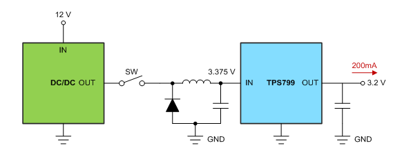
Figure 1: The TPS799 operating in dropout
Although it’s supposed to regulate 3.3V, the TPS799 does not have the headroom required to maintain regulation. As a result, the output voltage begins to track the input voltage.
What determines dropout?
The architecture of the LDO primarily determines dropout. To see why, let’s look at PMOS and NMOS LDOs and compare their operation.
PMOS LDO
Figure 2 shows a PMOS LDO architecture. In order to regulate the desired output voltage, the feedback loop controls the drain-to-source resistance, or RDS. As VIN approaches VOUT(nom), the error amplifier will drive the gate-to-source voltage, or VGS, more negative in order to lower RDS and maintain regulation.
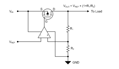
Figure 2: A PMOS LDO
At a certain point, however, the error-amplifier output will saturate at ground and cannot drive VGS more negative. RDS has reached its minimum value. Multiplying this RDS value against the output current, or IOUT, will yield the dropout voltage.
Bear in mind that the more negative the value of VGS, the lower RDS achieved. By increasing the input voltage, you can achieve a more negative VGS. Therefore, PMOS architectures will have lower dropout at higher output voltages. Figure 3 illustrates this behavior.
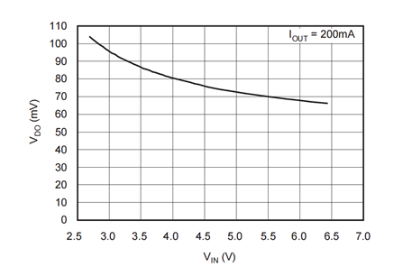
Figure 3: Dropout voltage vs. input voltage for the TPS799
As shown in Figure 3, the TPS799 has a lower dropout voltage as the input voltage (and output voltage, for that matter) increases. That is because a higher input voltage yields a more negative VGS.
NMOS LDO
In the case of an NMOS architecture, as shown in Figure 4, the feedback loop still controls RDS. As VIN approaches VOUT(nom), however, the error amplifier will increase VGS in order to lower the RDS and maintain regulation.
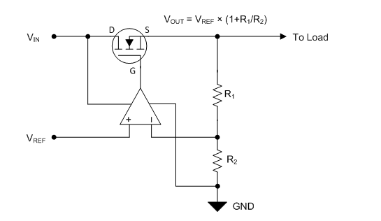
Figure 4: An NMOS LDO
At a certain point, VGS cannot increase any more, since the error-amplifier output will saturate at the supply voltage, or VIN. When this condition is met, RDSis at its minimum value. Multiplying this value against the output current, or IOUT, derives the dropout voltage.
This presents a problem though, because as VIN approaches VOUT(nom), VGS will also decrease, since the error-amplifier output saturates at VIN. This prevents ultra-low dropout.
Biasing the LDO
Many NMOS LDOs employ an auxiliary rail known as a bias voltage, or VBIAS, as shown in Figure 5.

Figure 5: An NMOS LDO with a bias rail
This rail serves as the positive supply rail for the error amplifier and allows its output to swing all the way up to VBIAS, which is higher than VIN. This type of configuration enables the LDO to maintain a high VGS, and therefore achieve ultra-low dropout at low output voltages.
Sometimes an auxiliary rail is not available but low dropout at a low output voltage is still desired. In such a situation, an internal charge pump can be substituted in place of VBIAS, as shown in Figure 6.

Figure 6: An NMOS LDO with an internal charge pump
The charge pump will boost VIN so that the error amplifier may generate a larger VGS value despite the lack of an external VBIAS rail.
Other variables
In addition to architecture, dropout is also affected by a few other variables, as outlined in Table 1.

Table 1: Variables affecting dropout
It’s clear that dropout is not a static value. Rather than just complicating your LDO choice, though, these variables should help you choose the optimal LDO for your specific set of conditions. Learn more about LDO dropout in the application note, Understanding LDO Dropout.


No comments